- jwebb's home page
- Posts
- 2019
- 2018
- 2017
- 2016
- 2015
- 2014
- 2013
- November (1)
- October (1)
- September (1)
- July (1)
- June (1)
- April (1)
- March (3)
- February (1)
- January (1)
- 2012
- 2011
- December (2)
- September (3)
- August (5)
- July (6)
- June (6)
- May (1)
- April (5)
- March (5)
- February (2)
- January (2)
- 2010
- December (3)
- October (3)
- September (2)
- August (2)
- June (2)
- May (4)
- April (4)
- March (2)
- February (4)
- January (10)
- 2009
- 2008
- 2007
- 2006
- July (1)
- My blog
- Post new blog entry
- All blogs
Rough cut of EEMC SMD spacer geometry

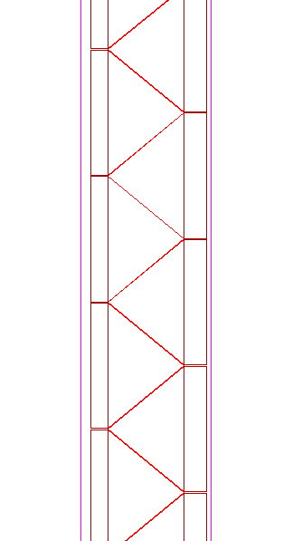
2.0 Implementation of the SMD spacers
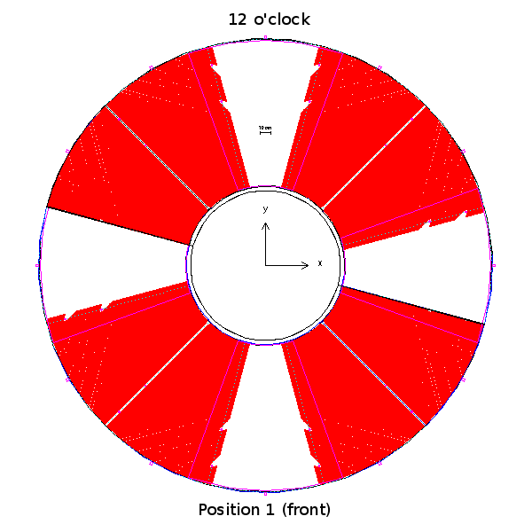
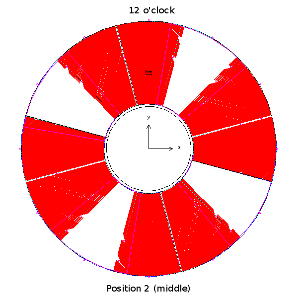
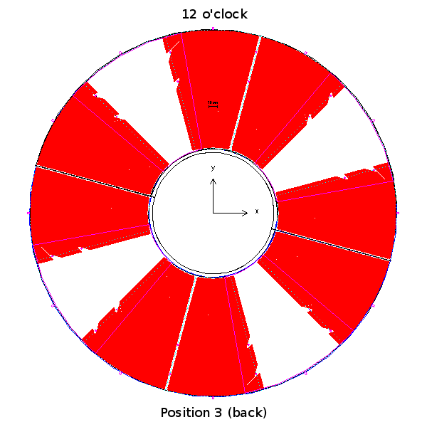
Spacers are setup to occupy the space unoccupied by the SMD planes. The spacers are setup to extend +/- 5 degrees into the neighboring sectors. By creating the SMD strips with the kONLY='MANY' option, the SMD strips will be given priority when geant performs tracking. (i.e. the spacer will be cut out to follow the shape defined by the SMD strips.)
The magenta lines below indicate the start and end of the SMD spacers.
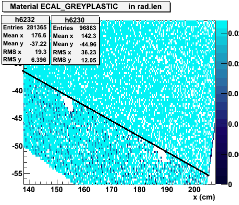
3.0 First look at materials observed by a geantino scan
Van Gough would be proud. The ears in the spacer appear to be cut off. Histogram 6230 should be the number of radiation lengths in the front material on the SMD. 6232 the "grey plastic" defined for the spacer. (In both cases, these are just copies of poly). The solid line shows the break point between spacer and SMD.
1) The spacer does not appear in the volume occupied by the SMD strips, as should be the case.
2) The spacer does not appear in the vacant region of the cut out. This is not as intended.
- jwebb's blog
- Login or register to post comments
